PCB Fabrication

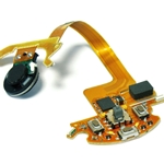
Partnering with Interactive Tech Solutions means you will be Simplifying, Consolidating, Reducing Cost and Time in the fabrication of printed circuit boards. Our PCB Fabrication direct partnerships provide Interactive Tech Solutions with the largest PCB footprint in the world. From our Quick-turn High Tech local USA factories to our low cost region Simple to High Tech factories in Taiwan, Malaysia and China. Our state-of-the art facilities can produce PCBs from 2-68 layers, with multiple laminations, HDI technologies, Flexible and Rigid-Flex PCB, backplane, hybrid material stack-up and Any-layer-Via structure with panel size up to 30X54 inches.

PCB Fabrication Assembly - Interactive Tech Solutions

PCB FAB Services and Capabilities

  • Quick Turn Services 24 hrs. – 5 Working Days
  • Asia Lead Times 5 – 30 Working Days
  • Rigid, Flex and Rigid-Flex Capabilities
  • High Density Backplane
  • Aluminum & Copper Base Materials
  • 2 to 68 Layers
  • Panel Size up to 30’’ X 54”
  • HDI PCB: Stacked Micro-via – Via in Pad
  • 0.2 mm Pitch BGA
  • Laser Via Structure
  • Copper & Epoxy Hole Fill
  • Mass production Heavy Copper up to 6 OZ
  • Advanced Thermal Solutions: Coin in Cavity and Copper Weight up 30oz on sample runs
  • Multiple Sequential Lamination
  • Aspect Ratio: 25:1
  • FR-4 to Exotic Materials
  • Cost Reduction Programs
  • Schedule Deliveries
  • Build to Stock Program
  • IPC – Class 2 & 3
  • UL, RoHS and REACH Certified
  • ISO 13485, AS 9100, IATF 16949 & NADCAP
  • Highly Certified Staff in Lean Six Sigma